Custom CMOS image sensor design on a budget
Specialised Imaging Ltd reports on the recent market launch of SI Sensors (Cambridge, UK) - a new division of the company focused on the development of advanced CMOS image sensors.
Drawing upon a team of specialists with a broad range of experience in image sensor design – SI Sensors is creating custom image sensor designs with cutting edge performance. In particular, the company’s in-house experts have specialist knowledge of visible and non-visible imaging technologies, optimised light detection and charge transfer, radiation-hard sensor design, and creating CCD-in-CMOS pixels to enable novel imaging techniques such as ultra-fast burst mode imaging.
Philip Brown, General Manager of SI Sensors said, “In addition to developing new sensors for Specialised Imaging’s next generation of ultra-fast imaging cameras utilising the latest foundry technologies, we are developing solutions for other customers with unique image sensor design requirements including for space and defence applications”.
He added “SI Sensors team also use their skills and experience to develop bespoke image sensor packages that accommodate custom electrical, mechanical, and thermal interface requirements. Our aim is always to achieve the best balance between image sensor performance and cost (optimised value) for customers. To ensure performance and consistent quality and reliability we perform detailed electro-optical testing from characterisation through to mass production testing adhering to industry standards such as EMVA 1288”.
For further information on custom CMOS image sensor design and production please visit www.si-sensors.com or contact SI Sensors on +44-1442-827728 or info@si-sensors.com.
Specialised Imaging Ltd is a dynamic company focused on niche imaging markets and applications, with particular emphasis on high-speed image capture and analysis. Drawing upon over 20 years’ experience, Specialised Imaging Ltd today are market leaders in the design and manufacture of ultra-fast framing cameras and ultra high-speed video cameras.
Monday, May 13, 2024
SI Sensors introduces custom CIS design services
Friday, May 10, 2024
NASA develops a 36 pixel sensor
From PetaPixel: https://petapixel.com/2024/04/30/nasa-develops-tiny-yet-mighty-36-pixel-sensor/
NASA Develops Tiny Yet Mighty 36-Pixel Sensor
While NASA’s James Webb Space Telescope is helping astronomers craft 122-megapixel photos 1.5 million kilometers from Earth, the agency’s newest camera performs groundbreaking space science with just 36 pixels. Yes, 36 pixels, not 36 megapixels.
The X-ray Imaging and Spectroscopy Mission (XRISM), pronounced “crism,” is a collaboration between NASA and the Japan Aerospace Exploration Agency (JAXA). The mission’s satellite launched into orbit last September and has been scouring the cosmos for answers to some of science’s most complex questions ever since. The mission’s imaging instrument, Resolve, has a 36-pixel image sensor.
This six-by-six pixel array measures 0.2 inches (five millimeters) per side, which is not so different from the image sensor in the Apple iPhone 15 and 15 Plus. The main camera in those smartphones is eight by six millimeters, albeit with 48 megapixels. That’s 48,000,000 pixels, just a handful more than 36.
How about a full-frame camera, like the Sony a7R V, the go-to high-resolution mirrorless camera? That camera has over 60 megapixels and captures images that are 9,504 by 6,336 pixels. The image sensor has a total of 60,217,344 pixels, 1,672,704 times the number of pixels in XRISM’s Resolve imager.
At this point, it is reasonable to wonder, “What could scientists possibly see with just 36 pixels?” As it turns out, quite a lot.
Resolve detects “soft” X-rays, which are about 5,000 times more energetic than visible light wavelengths. It examines the Universe’s hottest regions, largest structures, and most massive cosmic objects, like supermassive black holes. While it may not have many pixels, its pixels are extraordinary and can produce a rich spectrum of visual data from 400 to 12,000 electron volts.
“Resolve is more than a camera. Its detector takes the temperature of each X-ray that strikes it,” explains Brian Williams, NASA’s XRISM project scientist at Goddard. “We call Resolve a microcalorimeter spectrometer because each of its 36 pixels is measuring tiny amounts of heat delivered by each incoming X-ray, allowing us to see the chemical fingerprints of elements making up the sources in unprecedented detail.”
Put another way, each of the sensor’s 36 pixels can independently and accurately measure changes in temperature of specific wavelengths of light. The sensor measures how the temperature of each pixel changes based on the X-ray it absorbs, allowing it to measure the energy of a single particle of electromagnetic radiation.
There is a lot of information in this data, and scientists can learn an incredible amount about very distant objects based using these X-rays.
Resolve can detect particular wavelengths of light so precisely that it can detect the motions of individual elements within a target, “effectively providing a 3D view.” The camera can detect the flow of gas within distant galaxy clusters and track how different elements behave within the debris of supernova explosions.
The 36-pixel image sensor must be extremely cold during scientific operations to pull off this incredible feat.
Videographers may attach a fan to their mirrorless camera to keep it cool during high-resolution video recording. However, for an instrument like Resolve, a fan just won’t cut it.
Using a six-stage cooling system, the sensor is chilled to -459.58 degrees Fahrenheit (-273.1 degrees Celsius), which is just 0.09 degrees Fahrenheit (0.05 degrees Celsius) above absolute zero. By the way, the average temperature of the Universe itself is about -454.8 degrees Fahrenheit (-270.4 degrees Celsius).
While a 36-pixel camera helping scientists learn new things about the cosmos may sound unbelievable, “It’s actually true,” says Richard Kelley, the U.S. principal investigator for XRISM at NASA’s Goddard Space Flight Center in Greenbelt, Maryland.
“The Resolve instrument gives us a deeper look at the makeup and motion of X-ray-emitting objects using technology invented and refined at Goddard over the past several decades,” Kelley continues.
XRISM and Resolve offer the most detailed and precise X-ray spectrum data in the history of astrophysics. With just three dozen pixels, they are charting a new course of human understanding through the cosmos (and putting an end to the megapixel race).
Talk on Digital Camera Myths and Misunderstandings - Part II
In a follow-up to the talk that was previously shared on this blog, here's Digital Camera Myths, Misstatements and Misunderstandings Part II, a presentation by Wayne Prentice to Rochester, NY chapter of IS&T (Society for imaging Science and Tech.) on 17 April. 2024.
00:00 - Introduction
5:51 - Revisiting ISO sensitivity
9:12 - 12 ISO 10/Ha - really independent of camera and illuminant?
13:49 - "It's official: ISO 51,200 is the new 6400". Really?
22:44 - RCCB (Red, clear, clear Blue) sensors yield better SNR. Really?
25:35 - Depth of field: should you always use a longer focal length?
28:18 - sRGB, gamma, CRT display, and Human Vision
31:00 - Questions
Tuesday, May 07, 2024
NIT announces new full HD SWIR sensor - NSC2101
New High-Resolution, SWIR Sensor with High Performance
NIT (New Imaging Technologies) introduces its latest innovation in SWIR imaging technology: a high-resolution Short-Wave Infrared (SWIR) InGaAs sensor designed for the most demanding challenges in the field.
Overview
The new SWIR sensor – NSC2101 boasts remarkable features, including a high-performance InGaAs sensor with an 8µm pixel pitch, delivering an impressive 2MPIX resolution at 1920x1080px. Its ultra-low noise of only 25e- ensures exceptional image clarity, even in challenging environments. Additionally, with a dynamic range of 64dB, the sensor captures a wide spectrum of light intensities with precision and accuracy.
• 0.9µm to 1.7µm spectrum
• 2MPix – 1920x1080px @8µm pixel pitch
• 25e- readout noise
• 64dB dynamic range
This cutting-edge sensor is designed and manufactured by NIT in France and promises unparalleled performance and reliability. Leveraging advanced technology and expertise, NIT has crafted a sensor that meets the rigorous standards of ISR applications, offering crucial insights and intelligence in various scenarios.
Image examples


Applications
The applications of this SWIR sensor are vast and
diverse, catering to the needs of defense, security, and surveillance
industries. The sensor’s capabilities are indispensable for enhancing
situational awareness and decision-making, from monitoring border
security to providing critical intelligence in tactical operations.
Extension
Moreover,
NIT’s commitment to innovation extends beyond the sensor itself. The
camera version, integrating the NSC2101 sensor, will be released soon,
this summer
Monday, May 06, 2024
Job Postings - Week of 5 May 2024
|
UC Santa Cruz Systems Design and Characterization Engineer |
Santa Cruz, California, USA |
|
|
FAPESP - São Paulo Research Foundation Young Investigator Position in Quantum Technologies |
São Paulo, Brazil |
|
|
Apple Pixel Development Engineer |
Cupertino, California, USA |
|
|
Meta – Facebook App Sensor Application Engineer |
Sunnyvale, California, USA Redmond, Washington, USA |
|
|
University of Houston Postdoctoral/Senior Research Scientist-X-ray, photon counting detectors |
Houston, Texas, USA |
|
|
IRFU Staff position in detector physics at CEA/IRFU/DEDIP |
Saclay, France |
|
|
NASA Development of infrared detectors and focal plane arrays for space instruments |
Pasadena, California, USA |
|
|
Forvia-Faurecia ADAS Camera Systems Engineer |
Northville, Michigan, USA |
|
|
University of Edinburgh Sensor and Imaging Systems MSc |
Edinburgh, Scotland, UK |
Friday, May 03, 2024
Foveon sensor development "still in design stage"
https://www.dpreview.com/interviews/6004010220/sigma-full-frame-foveon
Full-frame Foveon sensor "still at design stage" says Sigma CEO, "but I'm still passionate"
"Unfortunately, we have not made any significant progress since last year," says Sigma owner and CEO Kazuto Yamaki, when asked about the planned full-frame Foveon camera. But he still believes in the project and discussed what such a camera could still offer.
"We made a prototype sensor but found some design errors," he says: "It worked but there are some issues, so we re-wrote the schematics and submitted them to the manufacturer and are waiting for the next generation of prototypes." This isn't quite a return to 'square one,' but it means there's still a long road ahead.
"We are still in the design phase for the image sensor," he acknowledges: "When it comes to the sensor, the manufacturing process is very important: we need to develop a new manufacturing process for the new sensor. But as far as that’s concerned, we’re still doing the research. So it may require additional time to complete the development of the new sensor."
The Foveon design, which Sigma now owns, collects charge at three different depths in the silicon of each pixel, with longer wavelengths of light able to penetrate further into the chip. This means full-color data can be derived at each pixel location rather than having to reconstruct the color information based on neighboring pixels, as happens with conventional 'Bayer' sensors. Yamaki says the company's thinking about the benefits of Foveon have changed.
"When we launched the SD9 and SD10 cameras featuring the first-generation Foveon sensor, we believed the biggest advantage was its resolution, because you can capture contrast data at every location. Thus we believed resolution was the key." he says: "Today there are so many very high pixel-count image sensors: 60MP so, resolution-wise there’s not so much difference."
But, despite the advances made elsewhere, Yamaki says there's still a benefit to the Foveon design "I’ve used a lot of Foveon sensor cameras, I’ve taken a bunch of pictures, and when I look back at those pictures, I find a noticeable difference," he says. And, he says, this appeal may stem from what might otherwise be seen as a disadvantage of the design.
"It could be color because the Foveon sensor has lots of cross-talk between R, B and G," he suggests: "In contrast, Bayer sensors only capture R, B and G, so if you look at the spectral response a Bayer sensor has a very sharp response for each color, but when it comes to Foveon there’s lots of crosstalk and we amplify the images. There’s lots of cross-talk, meaning there’s lots of gradation between the colors R, B and G. When combined with very high resolution and lots of gradation in color, it creates a remarkably realistic, special look of quality that is challenging to describe."
The complexity of separating the color information that the sensor has captured is part of what makes noise such a challenge for the Foveon design, and this is likely to limit the market, Yamaki concedes:
"We are trying to make our cameras with the Foveon X3 sensor more user-friendly, but still, compared to the Bayer sensor cameras, it won’t be easy to use. We’re trying to improve the performance, but low-light performance can’t be as good as Bayer sensor. We will do our best to make a more easy-to-use camera, but still, a camera with Foveon sensor technology may not be the camera for everybody."
But this doesn't dissuade him. "Even if we successfully develop a new X3 sensor, we may not be able to sell tons of cameras. But I believe it will still mean a lot," he says: "despite significant technology advancements there hasn't been much progress in image quality in recent years. There’s a lot of progress in terms of burst rate or video functionality, but whe
n you talk just about image quality, about resolution, tonality or dynamic range, there hasn’t been so much progress."
"If we release the Foveon X3 sensor today and people see the quality, it means a lot for the industry, that’s the reason I’m still passionate about the project."
Wednesday, May 01, 2024
Nexchip mass produces 55nm and 90nm BSI CIS
Google translation of a news article:
Jinghe integrates 50-megapixel image sensors into mass production and plans to double its CIS production capacity within the year
According to Jinghe Integration news, after the mass production of 90nm CIS and 55nm stacked CIS, Jinghe Integration (688249) CIS has added new products. Recently, Jinghe's integrated 55nm single-chip, 50-megapixel back-illuminated image sensor (BSI) has entered mass production, greatly empowering different application scenarios of smartphones and achieving a leapfrog move from mid- to low-end to mid-to-high-end applications. Jinghe Integration plans to see a doubling of CIS production capacity this year, and its share of shipments will increase significantly, becoming the second largest product axis after display driver chips.
Nexchip's website shows the following technologies.
https://www.nexchip.com.cn/en-us/Service/Roadmap

Monday, April 29, 2024
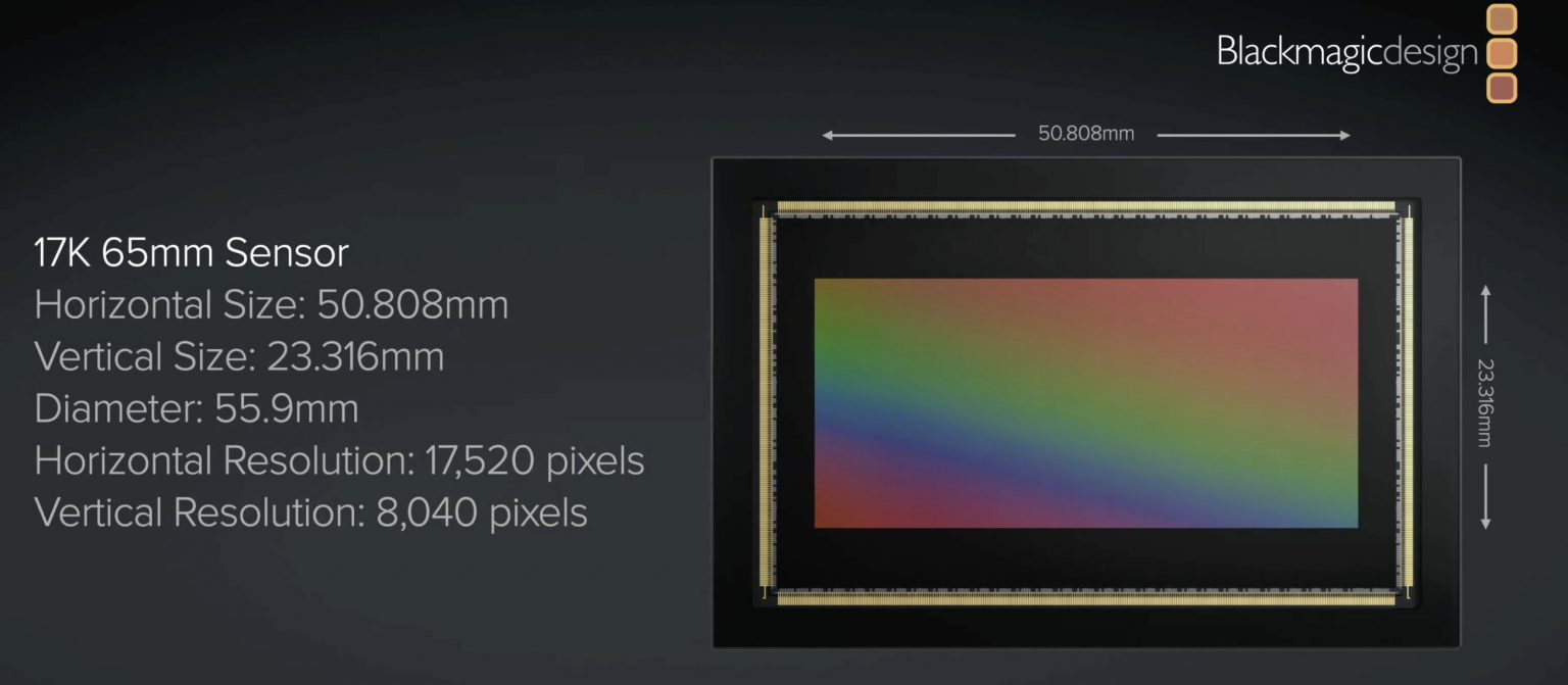
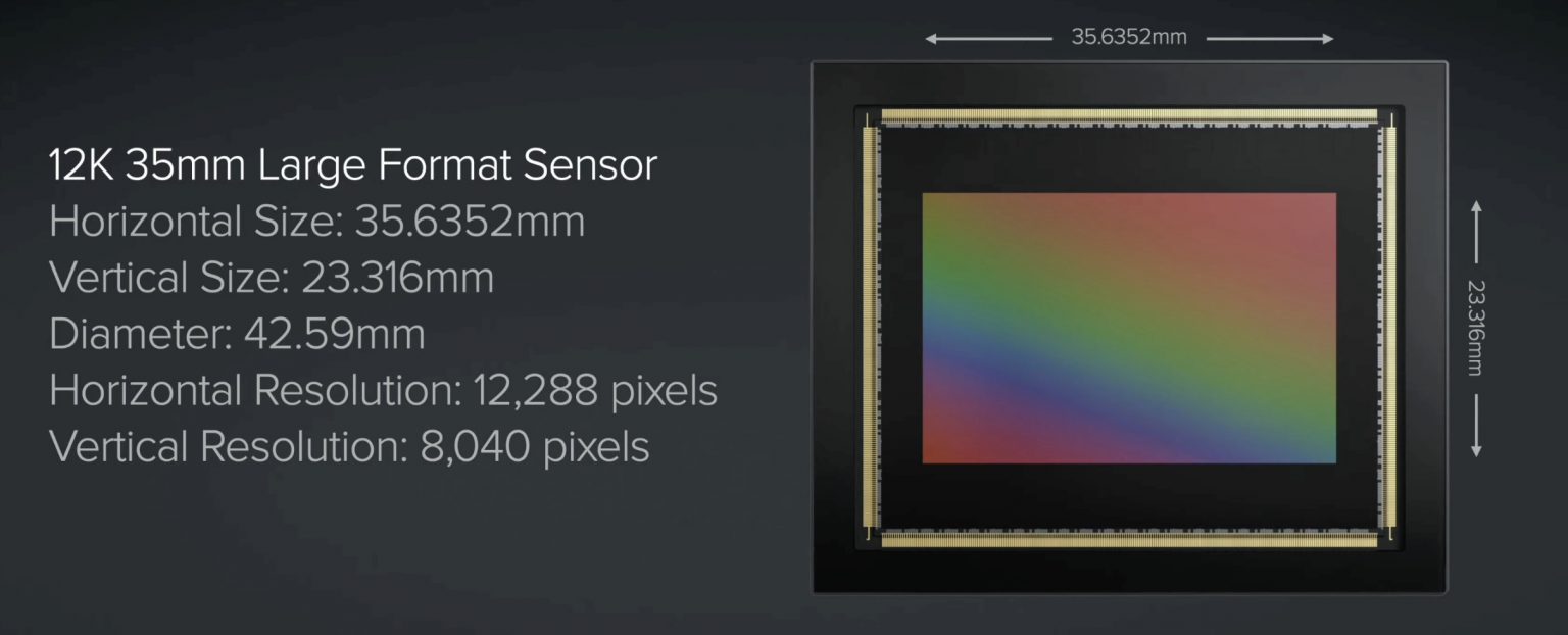
Blackmagic releases new 12K and 17K cine cameras
From: https://www.newsshooter.com/2024/04/12/blackmagic-design-ursa-cine-ursa-cine-17k/
Blackmagic Design URSA Cine & URSA Cine 17K

Sunday, April 28, 2024
Airy3D - Teledyne e2v collaboration
Link: https://www.airy3d.com/airy3d-e2v-collaboration/
Teledyne e2v and Airy3D collaboration delivers more affordable 3D vision solutions
Grenoble, FRANCE, April 23, 2024 —Teledyne e2v, a Teledyne Technologies [NYSE: TDY] company and global innovator of imaging solutions, is pleased to announce a new technology and design collaboration with Airy3D (Montreal, Canada), a leading 3D vision solution provider. The first result of this partnership is the co-engineering of the recently announced Topaz5D™, a low-cost, low power, passive, 2 megapixel global shutter sensor which produces 2D images and 3D depth maps.
Arnaud Foucher, Business Team Director at Teledyne e2v, said, “We’re very excited to have collaborated with Airy3D on the development of Topaz5D, our latest unique CMOS sensor. The need to deploy alternative 3D vision solutions in different industries is crucial. Teledyne e2v’s image sensor design capability coupled with Airy3D’s proven 3D technology has allowed us to develop more 3D vision products for several market segments with a reduced cost of ownership.”
Chris Barrett, CEO of Airy3D, commented, “Airy3D uniquely combines our patented optically Transmissive Diffraction Mask (TDM) design and deep software processing know-how, enabling our partners to add value to their products. Teledyne e2v’s image sensor design, production and supply chain expertise are paramount in introducing these novel 3D solutions to the market and this initiative is a key milestone for us.”
A Topaz5D Evaluation Kit and monochrome and color sensor samples are available now for evaluations and design. Please contact Teledyne e2v for more information.
Friday, April 26, 2024
Lecture on Noise in Event Cameras and "SciDVS" camera
Talk title: "Noise Limits of Event Cameras" presented at the Cambridge Huawei Frontiers in image Sensing 2024
Speaker: Prof. Tobi Delbruck
Abstract: "Cameras that mimic biological eyes have a 50 year history and the DVS event camera pixel is now nearly 20 years old. Event camera academic and industrial development is active, but it is only in the last few years that we understand more about the ultimate limits on their noise performance. This talk will be about those limits: What are the smallest changes that we can detect at a particular light intensity and particular speed? What are the main sources of noise in event cameras and what are the limits on these? I will discuss these results in the context of our PhD student Rui Graca’s work on SciDVS, a large-pixel DVS that targets scientific applications such as neural imaging and space domain awareness."